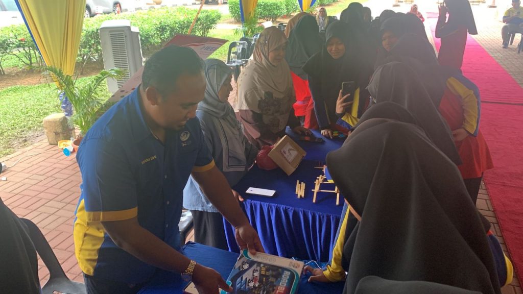
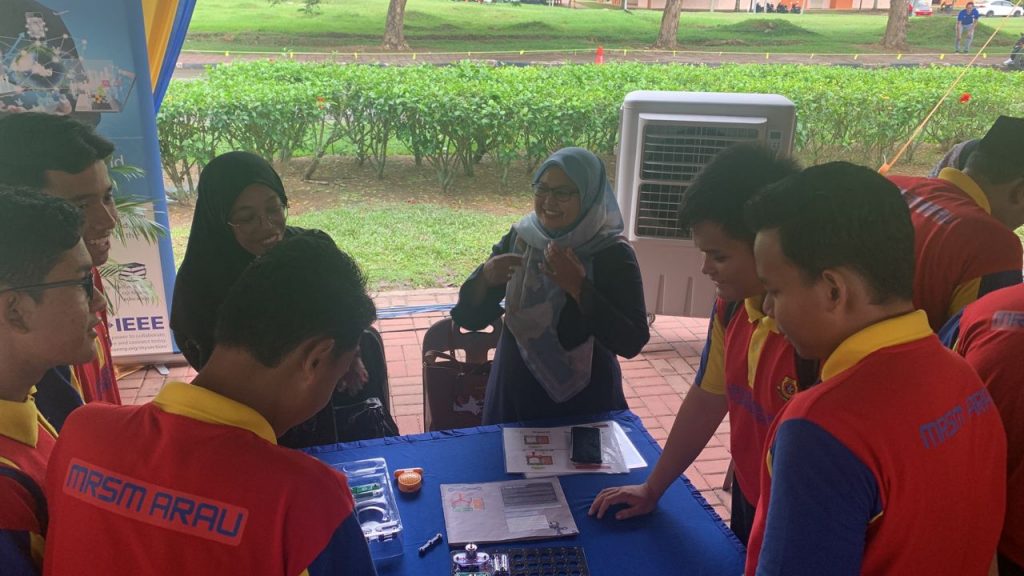
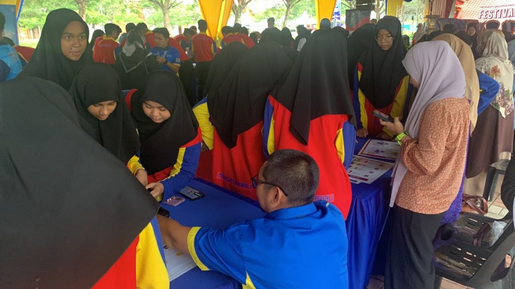
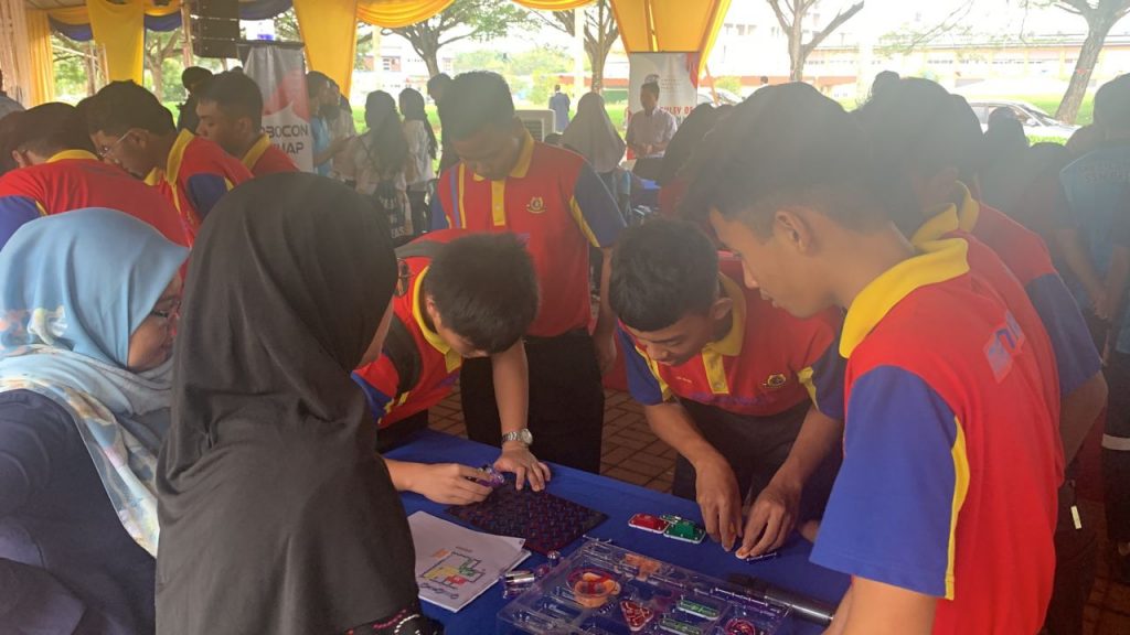
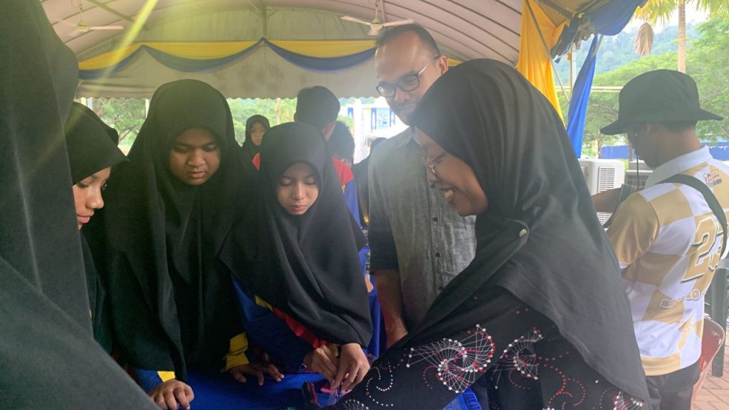
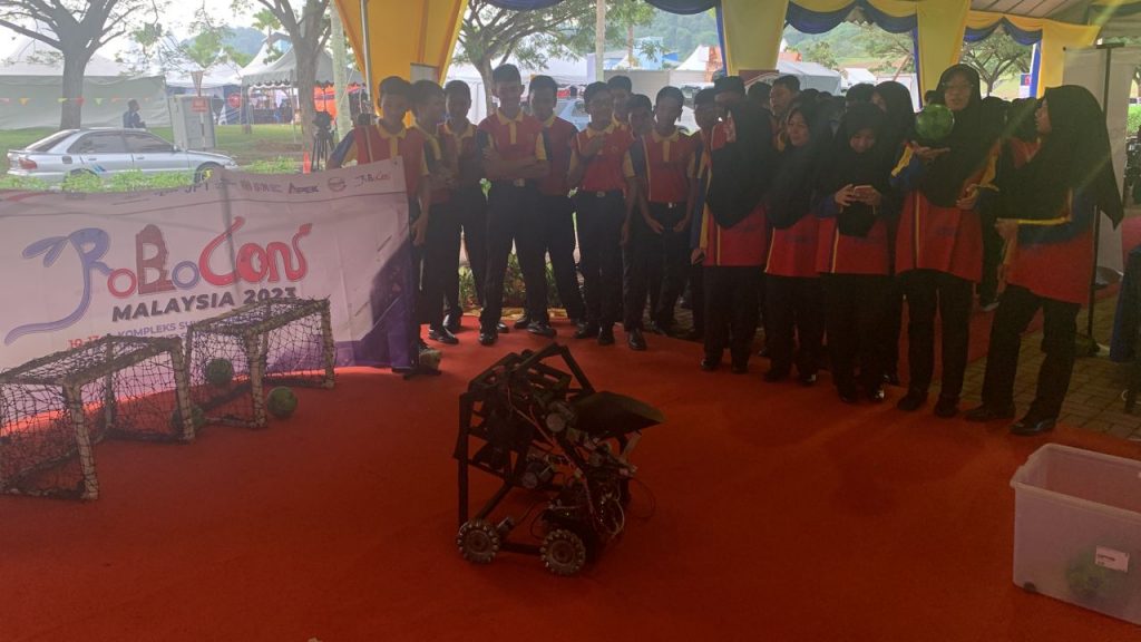
On November 21, 2023, several staff members from the Institute of Nano Electronic Engineering (INEE) were involved in the success of STEM with Community as part of the UniMAP Convocation Festival (FESTKON UniMAP 2023).
Institute of Nano Electronic Engineering
Universiti Malaysia Perlis
By Editor
On November 21, 2023, several staff members from the Institute of Nano Electronic Engineering (INEE) were involved in the success of STEM with Community as part of the UniMAP Convocation Festival (FESTKON UniMAP 2023).


By Editor
Abstract – Silicon-on-Insulator (SOI) technology provides a solution for controlling Short-Channel Effects (SCEs) and enhancing the performance of Metal-Oxide-Semiconductor Field-Effect Transistors (MOSFETs). However, scaling down SOI MOSFETs to a nanometer scale does not necessarily yield further scaling benefits. Introducing multiple gates, such as a double gate configuration, can effectively mitigate SCEs. Nonetheless, fabricating a flawless double gate structure is an exceedingly challenging endeavor that remains unrealized. The adoption of a back gate bias, with an asymmetrical thickness arrangement between the front and back gates, mimicking the behavior of a double gate, offers an alternative approach. This approach has the potential to modify the electrical characteristics of the device, thus potentially leading to improved control over SCEs. In this study, we employed 2D simulations using Atlas to investigate the influence of back gate biases, namely, -2.0 V, 0 V, and 2.0 V on a 10 nm silicon thickness at the top and a 20 nm buried oxide thickness for n-channel MOSFETs. We focused on key parameters, including threshold voltage (VTh), Drain Induced Barrier Lowering (DIBL), and Subthreshold Swing (SS). The results demonstrate that a negative back gate bias is the most favorable configuration, as it yields superior performance. This translates into more effectively controlled SCEs across all the parameters of interest.
Corresponding Author: Dr. Mohamad Faris Mohamad Fathil
Corresponding Author’s Email: mohamadfaris@unimap.edu.my
Download: PDF
Link to Publication: https://ijneam.unimap.edu.my/index.php/vol-16-no-4-october-2023
Institute of Nano Electronic Engineering, Universiti Malaysia Perlis
Lot 106, 108 & 110, Blok A, Taman Pertiwi Indah,
Jalan Kangar-Alor Setar, Seriab 01000 Kangar, Perlis, Malaysia
Tel: +604-979 8581 Fax: +604-979 8578 Email: webmaster.inee@unimap.edu.my